
1500V N-Channel Power MOSFET
$2.15100-999 Piece/Pieces
$1.85≥1000Piece/Pieces
| Payment Type: | L/C,T/T,Paypal |
| Incoterm: | FOB,CFR,CIF |
| Transportation: | Ocean,Air |
| Port: | SHANGHAI |

$2.15100-999 Piece/Pieces
$1.85≥1000Piece/Pieces
| Payment Type: | L/C,T/T,Paypal |
| Incoterm: | FOB,CFR,CIF |
| Transportation: | Ocean,Air |
| Port: | SHANGHAI |
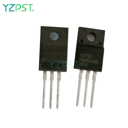
Model No.: YZPST-FM3N150C
Brand: YZPST
Place Of Origin: China
Vdss: 1500V
ID Continuous (Tc = 25 °C ): 1.8A
ID Continuous ( Tc = 100 °C ): 1.2A
Idm: 12A
Vgss: ±30V
EAS: 225mJ
Dv/dt: 5V/ns
| Selling Units | : | Piece/Pieces |
| Package Type | : | 1. Anti-electrostatic packaging 2. Carton box 3. Plastic protective packaging |
| Download | : |
|
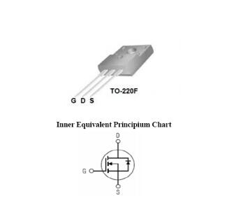
1500V N-Channel MOSFET
YZPST-FM3N150C
General Description
This Power MOSFET is produced using advanced self-aligned planar technology. This advanced technology has been especially tailored to minimize on-state resistance, provide superior switching performance, and withstand high energy pulse in the avalanche and commutation mode.
These devices can be used in various power switching circuit for system miniaturization and higher efficiency.
Features
3A, 1500V, RDS(on)typ. = 5Q@VGS = 10 V ld=1.5A
Low gate charge (typical9.3nC)
Low gate charge (typical2.4pf)
Fast switching
100% avalanche tested
Absolute Maximum Ratings Tc = 25 °C unless otherwise noted
| Symbol | Parameter | JFFM3N150C | Units | |
| Vdss | Drain - Source Voltage | 1500 | V | |
| Id | Drain Current | Continuous (Tc = 25 °C ) | 1.8 | A |
| Continuous ( Tc = 100 °C ) | 1.2 | A | ||
| Idm | Drain Current - Pulsed ( Note 1) | 12 | A | |
| Vgss | Gate - Source Voltage | ±30 | V | |
| EAS | Single Pulsed Avalanche Energy ( Note 2 ) | 225 | mJ | |
| dv/dt | Peak Diode Recovery dv/dt ( Note 3 ) | 5 | V/ns | |
| Pd | Power Dissipation (Tc = 25 °C ) | 30 | W | |
| Tj,Tstg | Operating and Storage Temperature Range | -55 to +150 | °C | |
| Tl | Maximum lead temperature for soldering purposes | 300 | °C | |
| 1/8 frome case for 5 seconds | ||||
Thermal characteristics
| Symbol | Parameter | JFFM3N150C | Units |
| Raic | Thermal Resistance, Junction-to-Case | 4.1 | °C/W |
| Rqja | Thermal Resistance, Junction-to-Ambient | 62.5 | °c/w |
Electrical Characteristics tc=25 °c unless otherwise noted
| Symbol | Parameter | Test Conditions | Min | Typ | Max | Units |
| Off Characteristics | ||||||
| BVdss | Drain - Source Breakdown Voltage | Vgs = 0 V, Id =250 uA | 1500 | V | ||
| / BVdss/ | Breakdown Voltage Temperature Coefficient | Id = 250 uA, Referenced to | -- | 1.3 | -- | v/°c |
| Tj | 25 °C | |||||
| Zero Gate Voltage Drain Current | Vds = 1500 V, Vgs = 0 V | 25 | uA | |||
| Idss | Vds = 1200 V, Tc = 125 °C | -- | -- | 500 | uA | |
| Igssf | Gate-Body Leakage Current, Forward | Vgs = 30 V, Vgs = 0 V | — | — | 100 | nA |
| Igssr | Gate-Body Leakage Current, Reverse | Vgs = -30 V, Vgs = 0 V | — | — | -100 | nA |
| On Characteristics | ||||||
| VGS(th) | Gate Threshold Voltage | Vds = Vgs, Id = 250 uA | 3 | — | 5 | V |
| RDS(on) | Static Drain-Source on-Resista nee | Vgs = 10 V, Id= 1.5A | — | 5 | 8 | Q |
| gFS | Forward Transconductance | Vds = 30 V, Id= 1.5 A ( Note | -- | 4.5 | -- | S |
| 4) | ||||||
| Dynamic Characteristics | ||||||
| Ciss | Input Capacitance | Vds = 25 V, Vgs = 0 V, f = | — | 1938 | — | pF |
| Coss | Output Capacitance | 1.0 MHz | — | 104 | — | pF |
| Crss | Reverse Transfer Capacitance | — | 2.4 | — | pF | |
| Rg | Gate resistance | F= 1.0 MHz | 3.5 | Q | ||
| Switching Characteristics | ||||||
| td(on) | Turn-On Delay Time | 34 | ns | |||
| tr | Turn-On Rise Time | Vds = 750 V, Id=3.0A/ Rg = | 17 | ns | ||
| td(off) | Turn-Off Delay Time | 100 , Vgs = 10 V (Note 4,5) | 56 | ns | ||
| tf | Turn-Off Fall Time | 27 | ns | |||
| Qe | Total Gate Charge | Vds = 750 V, Id =3.0 A Vgs = | 9.3 | nC | ||
| Qgs | Gate-Source Charge | 10 V (Note 4,5) | 15 | nC | ||
| Qgd | Gate-Drain Charge | 5.3 | nC | |||
| Drain - Source Diode Characteristics and Maximum Ratings | ||||||
| Is | Maximum Continuous Drain-Source Diode Forward Current | 3 | A | |||
| Ism | Maximum Pulsed Drain-Source Diode Forward Current | 12 | A | |||
| Vsd | Drain-Source Diode Forward Voltage | Vgs = 0 V, Is = 3.0 A | 1.5 | V | ||
| trr | Reverse Recovery Time | Vgs = 0 V, Is = 3.0 A | 302 | ns | ||
| Qrr | Reverse Recovery Charge | dlF/dt = 100 A/us ( Note | -- | 10 | -- | uC |
| 4) | ||||||
Notes:
1. Repetitive Rating : Pulsed width limited by maximum junction temperature
2. L= lO.OmH , Ias = 6.7A, Rg = 25Q, StartingTj = 25°C
3. Isd < 3.0Az di/dt < lOOA/us, Vdd < BVdss, Starting Tj = 25°C
4. Pulsed Test: Pulsed width <3OOusz Duty cycle < 2%
5. Essentially independent of operating temperature


Tel: 86-514-87782298
Whatsapp: +8613805278321
Address: 3rd Floor, Weiheng Building No.20 B Area, Yangzhou, Jiangsu China
Website: https://www.yzpst.com


Privacy statement: Your privacy is very important to Us. Our company promises not to disclose your personal information to any external company with out your explicit permission.
Fill in more information so that we can get in touch with you faster
Privacy statement: Your privacy is very important to Us. Our company promises not to disclose your personal information to any external company with out your explicit permission.