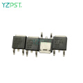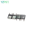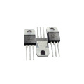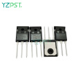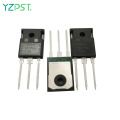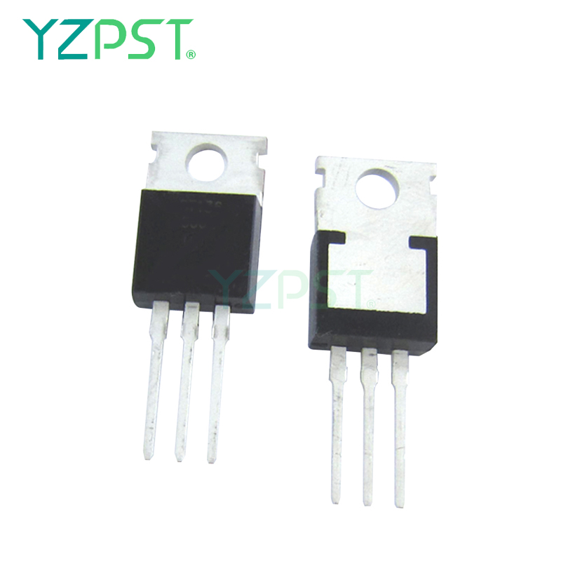
TO-220 scr phase control 25A Transistor 25TTS12
$0.252000-99999 Piece/Pieces
$0.22≥100000Piece/Pieces
| نوع پرداخت: | L/C,T/T,Paypal |
| اینکوترم: | FOB,CFR,CIF |
| حداقل سفارش: | 2000 Piece/Pieces |
| حمل و نقل: | Ocean,Air |
| بندر: | SHANGHAI |

$0.252000-99999 Piece/Pieces
$0.22≥100000Piece/Pieces
| نوع پرداخت: | L/C,T/T,Paypal |
| اینکوترم: | FOB,CFR,CIF |
| حداقل سفارش: | 2000 Piece/Pieces |
| حمل و نقل: | Ocean,Air |
| بندر: | SHANGHAI |
مدل شماره: YZPST-25TTS12
نام تجاری: YZPST
| فروش واحد | : | Piece/Pieces |
| نوع بسته بندی | : | 1. Anti-electrostatic packaging 2. Carton box 3. Plastic protective packaging |
Phase Control SCR, 25 A
DESCRIPTION/FEATURES
The 25TTS... High Voltage Series of silicon controlled rectifiers are specifically designed for medium power switching and phase control applications. The glass passivation technology used has reliable operation up to
125 °C junction temperature.
Typical applications are in input rectification (soft start) and these products are designed to be used with Vishay HPP input diodes, switches and output rectifiers which are available in identical package outlines.
This product has been designed and qualified for industrial level.

|
PRODUCT SUMMARY |
|
|
VT at 16 A |
< 1.25 V |
|
ITSM |
300 A |
|
VRRM |
800/1200 V |
|
OUTPUT CURRENT IN TYPICAL APPLICATIONS |
|||
|
APPLICATIONS |
SINGLE-PHASE BRIDGE |
THREE-PHASE BRIDGE |
UNITS |
|
Capacitive input filter TA = 55 °C, TJ = 125 °C, common heatsink of 1 °C/W |
18 |
22 |
A |
|
MAJOR RATINGS AND CHARACTERISTICS |
|||
|
PARAMETER |
TEST CONDITIONS |
VALUES |
UNITS |
|
IT(AV) |
Sinusoidal waveform |
16 |
A |
|
IRMS |
|
25 |
|
|
VRRM/VDRM |
|
800/1200 |
V |
|
ITSM |
|
300 |
A |
|
VT |
16 A, TJ = 25 °C |
1.25 |
V |
|
dV/dt |
|
500 |
V/µs |
|
dI/dt |
|
150 |
A/µs |
|
TJ |
|
- 40 to 125 |
°C |
|
VOLTAGE RATINGS |
|||
|
PART NUMBER |
VRRM, MAXIMUM PEAK REVERSE VOLTAGE V |
VDRM, MAXIMUM PEAK DIRECT VOLTAGE V |
IRRM/IDRM AT 125 °C mA |
|
25TTS08 |
800 |
800 |
10 |
|
25TTS12 |
1200 |
1200 |
|
|
ABSOLUTE MAXIMUM RATINGS |
||||||
|
PARAMETER |
SYMBOL |
TEST CONDITIONS |
VALUES |
UNITS |
||
|
TYP. |
MAX. |
|||||
|
Maximum average on-state current |
IT(AV) |
TC = 93 °C, 180° conduction half sine wave |
16 |
A |
||
|
Maximum RMS on-state current |
IRMS |
|
25 |
|||
|
Maximum peak, one-cycle, non-repetitive surge current |
ITSM |
10 ms sine pulse, rated VRRM applied |
300 |
|||
|
10 ms sine pulse, no voltage reapplied |
350 |
|||||
|
Maximum I2t for fusing |
I2t |
10 ms sine pulse, rated VRRM applied |
450 |
A2s |
||
|
10 ms sine pulse, no voltage reapplied |
630 |
|||||
|
Maximum I2√t for fusing |
I2√t |
t = 0.1 to 10 ms, no voltage reapplied |
6300 |
A2√s |
||
|
Maximum on-state voltage drop |
VTM |
16 A, TJ = 25 °C |
1.25 |
V |
||
|
On-state slope resistance |
rt |
TJ = 125 °C |
12.0 |
mΩ |
||
|
Threshold voltage |
VT(TO) |
1.0 |
V |
|||
|
Maximum reverse and direct leakage current |
IRM/IDM |
TJ = 25 °C |
VR = Rated VRRM/VDRM |
0.5 |
mA |
|
|
TJ = 125 °C |
10 |
|||||
|
Holding current |
IH |
Anode supply = 6 V, resistive load, initial IT = 1 A |
- |
100 |
||
|
Maximum latching current |
IL |
Anode supply = 6 V, resistive load |
200 |
|||
|
Maximum rate of rise of off-state voltage |
dV/dt |
|
500 |
V/µs |
||
|
Maximum rate of rise of turned-on current |
dI/dt |
|
150 |
A/µs |
||
|
TRIGGERING |
||||
|
PARAMETER |
SYMBOL |
TEST CONDITIONS |
VALUES |
UNITS |
|
Maximum peak gate power |
PGM |
|
8.0 |
W |
|
Maximum average gate power |
PG(AV) |
|
2.0 |
|
|
Maximum peak positive gate current |
+ IGM |
|
1.5 |
A |
|
Maximum peak negative gate voltage |
- VGM |
|
10 |
V |
|
Maximum required DC gate current to trigger |
IGT |
Anode supply = 6 V, resistive load, TJ = - 10 °C |
60 |
mA |
|
Anode supply = 6 V, resistive load, TJ = 25 °C |
45 |
|||
|
Anode supply = 6 V, resistive load, TJ = 125 °C |
20 |
|||
|
Maximum required DC gate voltage to trigger |
VGT |
Anode supply = 6 V, resistive load, TJ = - 10 °C |
2.5 |
V |
|
Anode supply = 6 V, resistive load, TJ = 25 °C |
2.0 |
|||
|
Anode supply = 6 V, resistive load, TJ = 125 °C |
1.0 |
|||
|
Maximum DC gate voltage not to trigger |
VGD |
TJ = 125 °C, VDRM = Rated value |
0.25 |
|
|
Maximum DC gate current not to trigger |
IGD |
2.0 |
mA |
|
|
SWITCHING |
||||
|
PARAMETER |
SYMBOL |
TEST CONDITIONS |
VALUES |
UNITS |
|
Typical turn-on time |
tgt |
TJ = 25 °C |
0.9 |
µs |
|
Typical reverse recovery time |
trr |
TJ = 125 °C |
4 |
|
|
Typical turn-off time |
tq |
110 |
||
|
THERMAL AND MECHANICAL SPECIFICATIONS |
|||||
|
PARAMETER |
SYMBOL |
TEST CONDITIONS |
VALUES |
UNITS |
|
|
Maximum junction and storage temperature range |
TJ, TStg |
|
- 40 to 125 |
°C |
|
|
Maximum thermal resistance, junction to case |
RthJC |
DC operation |
1.1 |
°C/W |
|
|
Maximum thermal resistance, junction to ambient |
RthJA |
|
62 |
||
|
Typical thermal resistance, case to heatsink |
RthCS |
Mounting surface, smooth and greased |
0.5 |
||
|
Approximate weight |
|
|
2 |
g |
|
|
0.07 |
oz. |
||||
|
Mounting torque |
minimum |
|
|
6 (5) |
kgf · cm (lbf · in) |
|
maximum |
|
|
12 (10) |
||
|
Marking device |
|
Case style TO-220AB |
25TTS08 |
||
|
25TTS12 |
|||||


تلفن: 86-514-87782298
Whatsapp: +8613805278321
نشانی: 3rd Floor, Weiheng Building No.20 B Area, Yangzhou, Jiangsu China
سایت اینترنتی: https://www.yzpst.com


بیانیه حفظ حریم خصوصی: حریم خصوصی شما برای ما بسیار مهم است. شرکت ما قول می دهد که اطلاعات شخصی شما را برای هرگونه مجوزهای صریح خود برای هرگونه گسترش فاش نکند.
اطلاعات بیشتری را پر کنید تا بتواند سریعتر با شما در تماس باشد
بیانیه حفظ حریم خصوصی: حریم خصوصی شما برای ما بسیار مهم است. شرکت ما قول می دهد که اطلاعات شخصی شما را برای هرگونه مجوزهای صریح خود برای هرگونه گسترش فاش نکند.