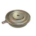

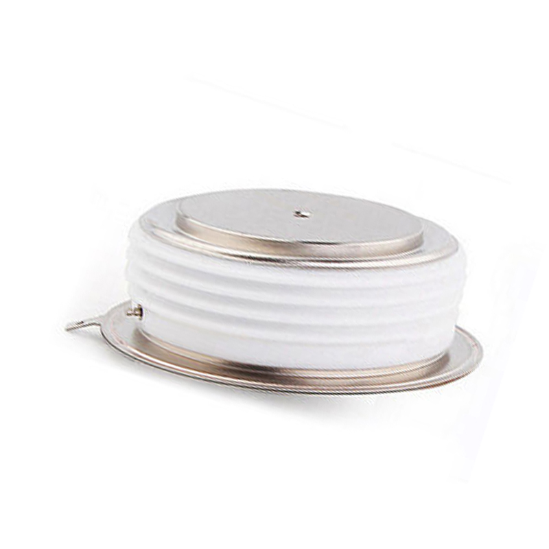
High dV/dt capability 6500V high power thyristor
$1501-99 Piece/Pieces
$95≥100Piece/Pieces
| Payment Type: | L/C,T/T,Paypal |
| Incoterm: | FOB,CFR,CIF |
| Min. Order: | 1 Piece/Pieces |
| Transportation: | Ocean,Air |
| Port: | SHANGHAI |

$1501-99 Piece/Pieces
$95≥100Piece/Pieces
| Payment Type: | L/C,T/T,Paypal |
| Incoterm: | FOB,CFR,CIF |
| Min. Order: | 1 Piece/Pieces |
| Transportation: | Ocean,Air |
| Port: | SHANGHAI |
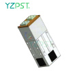
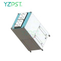
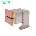
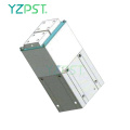
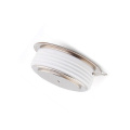
Model No.: YZPST-KP894A-6500V
Brand: YZPST
VRRM: 6500V
VRSM: 894A
| Selling Units | : | Piece/Pieces |
| Package Type | : | 1. Anti-electrostatic packaging 2. Carton box 3. Plastic protective packaging |
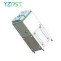
High Power Thyristor FOR PHASE CONTROL APPLICATIONS
YZPST-KP894A-6500V
Features:
. All Diffused Structure
. Interdigitated Amplifying Gate Configuration v
. Guaranteed Maximum Turn-Off Time
. High dV/dt Capability
. Pressure Assembled Device
ELECTRICAL CHARACTERISTICS AND RATINGS
Blocking - Off State
| VRRM (1) | VDRM (1) | VRSM (1) |
| 6500 | 6500 | 6600 |
VRRM = Repetitive peak reverse voltage
VDRM = Repetitive peak off state voltage
VRSM = Non repetitive peak reverse voltage (2)
| Repetitive peak reverse leakage and off state leakage | IRRM / IDRM | 20 mA 200 mA (3) |
| Critical rate of voltage rise | dV/dt (4) | 1000 V/msec |
Notes:
All ratings are specified for Tj=25 oC unless otherwise stated.
(1) All voltage ratings are specified for an applied
50Hz/60zHz sinusoidal waveform over the
temperature range -40 to +125 oC.
(2) 10 msec. max. pulse width
(3) Maximum value for Tj = 125 oC.
(4) Minimum value for linear and exponential waveshape to 80% rated VDRM. Gate open. Tj = 125 oC.
(5) Non-repetitive value.
(6) The value of di/dt is established in accordance with EIA/NIMA Standard RS-397, Section 5-2-2-6. The value defined would be in addition to that obtained from a ubber circuit,comprising a 0.2 mF capacitor and 20 ohmsresistance in parallel with the thristor under test.
Conducting - on state
| Parameter | Symbol | Min. | Max. | Typ. | Units | Conditions |
| Max. average value of on-state current | IT(AV)M |
| 894 |
| A | Sinewave,180o conduction,Tc=60oC |
| RMS value of on-state current | IT(RMS)m |
| 1404 |
| A | Nominal value |
| Peak one cPSTCle surge (non repetitive) current |
ITSM |
| -
12 |
| kA
kA | 8.3 msec (60Hz), sinusoidal wave- shape, 180o conduction, Tj = 125 oC 10.0 msec (50Hz), sinusoidal wave- shape, 180o conduction, Tj = 125 oC |
| I square t | I2t |
| 0.72x10⁶ |
| A2s | 8.3 msec |
| Latching current | IL |
| 3000 |
| mA | VD = 24 V; RL= 12 ohms |
| Holding current | IH |
| 300 |
| mA | VD = 24 V; I = 2.5 A |
| Peak on-state voltage | VTM |
| 2.4 |
| V | ITM = 1000 A ,Tj = 25 oC |
| Critical rate of rise of on-state current (5, 6) | di/dt |
| - |
| A/ms | Switching from VDRM £ 1000 V, non-repetitive |
| Critical rate of rise of on-state current (6) | di/dt |
| 200 |
| A/ms | Switching from VDRM £ 1000 V |

| Sym | A | B | C | D | H |
| mm | 75 | 47 | 66 | 3.5×3 | 26±1 |


Tel: 86-514-87782298
Whatsapp: +8613805278321
Address: 3rd Floor, Weiheng Building No.20 B Area, Yangzhou, Jiangsu China
Website: https://www.yzpst.com


Privacy statement: Your privacy is very important to Us. Our company promises not to disclose your personal information to any external company with out your explicit permission.
Fill in more information so that we can get in touch with you faster
Privacy statement: Your privacy is very important to Us. Our company promises not to disclose your personal information to any external company with out your explicit permission.