


Please Leave Us A Message
Privacy statement: Your privacy is very important to Us. Our company promises not to disclose your personal information to any external company with out your explicit permission.

 May 08, 2019
Advances in GaN technology have driven devices to operate at higher power, supply voltages, and frequencies.

As shown in Figure 1, Qorvo's QPD1013 transistor uses 0.50 μm GaN-on-SiC technology. It is available in a cost-effective 6.6x7.2 mm DFN (bilateral flat no-lead) package for simpler PCB assembly compared to traditional cermet packages.
Although Qorvo's GaN transistors are very efficient, considering the high RF power level means that even with a highly efficient PA, the transistors will have significant power consumption. Since the transistor is an SMT component, the PCB needs to be carefully designed to optimize thermal performance. Both methods have been evaluated and the results of both have been reported.
The first method uses an array of copper-clad holes under the ground pad of the transistor, and the second method uses copper coin technology. Copper coins are a solid piece of copper (commonly referred to as a metal block) that is embedded in the PCB during manufacture to allow efficient heat transfer from the transistor to the carrier on which the PCB is mounted. Many PCB manufacturers have experience in copper-clad technology, but the copper coin technology at RF frequencies is not yet mature.
Transistor measurementThis design uses large and small signal measurements of sample transistors assembled with a 20 mil thick Rogers RO4350. The transistor is statically biased to 65V, 240mA.
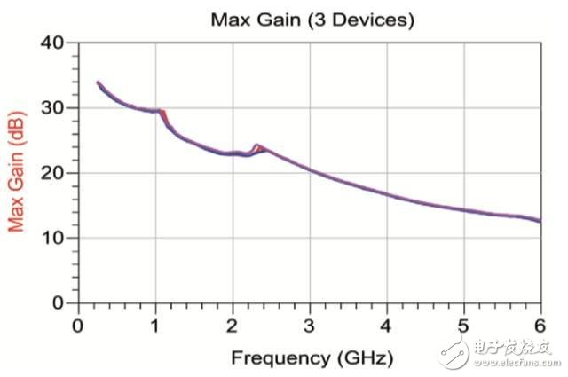
Figure 2 shows the maximum usable gain (MAG) of three different transistors as a function of frequency, which clearly shows very good inter-cell uniformity. Although the QPD1013 exhibits a gain of more than 6 GHz, it is best suited to operate up to about 3.5 GHz for practical reasons.
Maximum gain (3 devices) Maximum gain (dB) Frequency (GHz)
Load pull measurements show that when operating at 10% duty cycle and 100 μs pulse width, the transistor can deliver more than 52dBm 160 W) of RF output power with an efficiency of approximately 70%. This load pull data is used as the basis for PA large signal design.
Power amplifier designThe starting point for PA design is to make the transistor unconditionally stable throughout the operating frequency band. The stability within the band must first be ensured by incorporating an RC stable network at the RF input. The power consumed by the series resistor is too high for conventional SMT components, so high power aluminum nitride resistors from IMS are used. The amplifier needs to be unconditionally stable at all frequencies below -40 °C to allow the amplifier to operate over a wide temperature range. Low band stability can be greatly improved by adding appropriate RC decoupling at the bias feed point, which can be added later in the design process.
The initial load pull data provided by Qorvo is used to determine the optimum load impedance for output power and drain efficiency between 1.2 GHz and 1.8 GHz. The QPD1013 can deliver up to 200W under certain load conditions, but requires careful consideration of operating efficiency to ensure acceptable transistor operating temperatures. The load impedance resulting in the highest drain efficiency is chosen as the target impedance presented by the output matching network. The corresponding RF output power level is still high and the higher efficiency ensures acceptable thermal performance.
The output matching network utilizes a bandpass topology to meet the target load impedance. High operating voltages and high RF power levels pose a potential pitfall for careless designers. It is important to keep the RF track wide enough to avoid excessive temperature and potential damage due to very high RF power levels. The matching capacitor must be carefully chosen to have a sufficient breakdown voltage to withstand a DC and RF voltage swing with a sufficient amount of Q to avoid excessive power consumption and reduced efficiency.
The Keysight Momentum is used to perform planar EM simulation on the metal parts of the output matching network, and the multi-port S-parameter block is simulated by the embedded high-frequency model of the O805 SMT component. Figure 3 shows a hybrid EM/schematic diagram of the output matching network circuit.


The simulated load impedance is plotted against the target on the Smith chart normalized to 10 Ω in Figure 4. The simulated load curve is overlaid on the provided load traction profile (not shown) indicating that the target power and efficiency values will be met.
S(3,3) QPD1013_Opt_Zload_v1..S(1,1)
Frequency (1.200GHz to 1.9000GHz)
The analog insertion loss of the output network is shown in Figure 5.

The output matching network loss comes from transmission line losses and SMT component losses in the PCB media. At these output power levels, even a fraction of a dB loss will reach several watts of dissipated power, which significantly reduces overall PA efficiency.

Figure 6 EM analog input matching
The input matching network uses a low-pass architecture. IMS aluminum nitride resistors are used in the gate stability network. These can consume several watts of power, which allows the PA to withstand the high input drive levels of 10 to 20W required to operate the PA at P-3dB compression. Figure 6 shows the input matching network in the same way as the output matching network.
It can be seen that the layout of the input and output matching networks includes inductive loops and pads to adjust PA performance after manufacture. In the end, these are not needed, and the only post-manufacturing modification is a small change to the capacitance value.
The analog small signal performance of the PA is shown in Figure 7. Describes wide bandwidth and flat gain and frequency response.

The above is the Design and Implementation of GaN PA for SMT Transistors (Qorvo's QPD1013) we have listed for you. You can submit the following form to obtain more industry information we provide for you.
You can visit our website or contact us, and we will provide the latest consultation and solutions
Send Inquiry
Most Popular
lastest New
Send Inquiry
Tel: 86-514-87782298
Whatsapp: +8613805278321
Address: 3rd Floor, Weiheng Building No.20 B Area, Yangzhou, Jiangsu China
Website: https://www.yzpst.com
Privacy statement: Your privacy is very important to Us. Our company promises not to disclose your personal information to any external company with out your explicit permission.
Fill in more information so that we can get in touch with you faster
Privacy statement: Your privacy is very important to Us. Our company promises not to disclose your personal information to any external company with out your explicit permission.