Thyristors have many advantages, such as: low power control of high power, power amplification up to several hundred thousand times; extremely fast response, opening and closing in microseconds; no contact operation, no spark, no noise; high efficiency , low cost and so on. Therefore, especially in high-power UPS power supply systems, thyristors are widely used in rectifier circuits, static bypass switches, and non-contact output switches.
Thyristor weaknesses: static and dynamic overload capability is poor and susceptible to interference and misconnection.
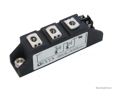
Thyristor classification from the appearance of the main: bolt-shaped, flat and flat bottom shape.
2 Ordinary thyristor structure and working principle Thyristor is PNPN four three-terminal device, a total of three PN junction. When analyzing the principle, it can be regarded as consisting of a PNP tube and an NPN tube. The equivalent diagram is shown in Fig. 1(a). Fig. 1(b) is the circuit symbol of the thyristor.
2.1 Thyristor Operation The thyristor is a four-layer three-terminal device. It has three PN junctions: J1, J2, and J3. The NP junction can be divided into two parts to form a composite
PNP Transistor and an NPN triode.
When the thyristor is subjected to a positive anode voltage, in order to make the thyristor conductive, the PN junction J2 that withstands reverse voltage must lose its blocking effect. The collector current of each transistor is at the same time the base current of the other transistor. Therefore, they are two mutually compounded transistor circuits. When sufficient gate current Ig flows in, a strong positive feedback is formed, causing saturation of the two transistors.
Let collector current of PNP tube and NPN tube be IC1 and IC2 respectively, emitter current corresponding to Ia and Ik, current amplification factor corresponding to α1=IC1/Ia and α2=IC2/Ik, set opposite phase of flow through J2 junction. The leakage current is ICO, and the anode current of the thyristor is equal to the sum of the collector current and leakage current of the two tubes:
If the gate current is Ig, the thyristor cathode current is: Ik=Ia+Ig.
Therefore, it can be concluded that the thyristor anode current is:
The current amplification factors α1 and α2 of the silicon PNP transistor and the silicon NPN transistor change drastically with changes in the emitter current thereof. When the thyristor is subject to a positive anode voltage and the gate is not receiving a voltage, Ig=0 ((α1+α2)) in equation (1) is very small, so the thyristor anode current Ia≈ICO, and the thyristor is in positive blocking State; when the thyristor is at the forward gate voltage, the current Ig flows from the gate G, because the sufficiently large Ig flows through the emitter junction of the NPN tube, thereby increasing the amplification factor α2, generating a sufficiently large collector current IC2 flowing through the PNP The emitter junction of the tube and the current amplification factor α1 of the PNP tube are increased, resulting in a larger collector current IC1 flowing through the emitter junction of the NPN tube, so that a strong positive feedback process proceeds rapidly.
When α1 and α2 increase as the emitter current makes (α1+α2)≈1, the denominator 1-(α1+α2)≈0 in equation (1) increases the anode current Ia of the thyristor. At this time, the current flowing through the thyristor is completely determined by the voltage of the main circuit and the loop resistance, and the thyristor is already in the forward conduction state. After the thyristor is turned on, 1-(α1+α2)≈0 in Equation (1), even if the gate current Ig=0, the thyristor can still maintain the original anode current Ia and continue conduction, and the gate has lost its effect. After the thyristor is turned on, if the power supply voltage is continuously reduced or the loop resistance is increased so that the anode current Ia decreases below the holding current IH, the thyristors return to the blocking state due to the rapid drop of α1 and α2.
2.2 Thyristor operating conditions Since the thyristor has only two operating states, on and off, it has switching characteristics. This feature requires certain conditions to convert. See Table 1 for the conditions.
(1) When the thyristor is subjected to a reversed anode voltage, the thyristor is turned off regardless of the voltage applied to the gate.
(2) When the thyristor is subjected to a positive anode voltage, the thyristor is turned on only when the gate is subjected to a forward voltage.
(3) When the thyristor is turned on, as long as there is a certain positive anode voltage, regardless of the gate voltage, the thyristor remains on, that is, the gate loses its function after the thyristor is turned on.
(4) Thyristor is turned off when the main circuit voltage (or current) is reduced to approximately zero when the thyristor is turned on.
3 thyristor voltage characteristics and the main parameters 3.1 thyristor volt-ampere characteristics thyristor A and cathode K between the voltage and the thyristor anode current relationship between the thyristor volt-ampere characteristics, as shown in Figure 2. The forward characteristic is in the first quadrant and the reverse characteristic is in the third quadrant.
(1) Reverse characteristics When the gate G is open and the anode is applied with a reverse voltage (see Figure 3), the J2 junction is forward biased, but the J1 and J2 junctions are reversed. At this point, only a small reverse saturation current can flow. When the voltage is further increased to the avalanche breakdown voltage of the J1 junction, the J3 junction also breaks down and the current rapidly increases, as shown in the characteristic curve OR of FIG. The voltage URO at the bend is called the "reverse transition voltage." After this, the thyristor will have a permanent reverse breakdown.
(2) Forward Characteristics When gate G is open and positive voltage is applied to anode A (see Figure 4), J1 and J3 are forward biased, but J2 is reverse biased. This is similar to the reverse characteristic of normal PN junction. Only a small current can flow, which is called the positive blocking state. When the voltage increases, the characteristic curve OA of FIG. 2 starts to curve, and the voltage UBO at the bending point is called “forward switching voltage”.
Since the voltage rises to the avalanche breakdown voltage of the J2 junction, an avalanche double effect occurs in the J2 junction, a large number of electrons and holes are generated in the junction region, electrons enter the N1 region, and holes enter the P2 region. Electrons entering the N1 region recombine with holes injected from the P1 region into the N1 region through the J1 junction. Similarly, holes entering the P2 region are combined with electrons injected into the P2 region from the N2 region through the J3 junction. After the avalanche breakdown, the electrons entering the N1 region and the holes entering the P2 region are not completely recombined. In this case, electrons are accumulated in the N1 region, and holes are accumulated in the P2 region. As a result, the potential of the P2 region increases, the potential of the N1 region decreases, and the J2 junction becomes a positive bias. As long as the current slightly increases, the voltage rapidly increases. Falling, there is the so-called negative resistance characteristics, see the dashed line AB in Figure 2. At this time, the three junctions J1, J2, and J3 are all in forward bias, and the thyristor enters the forward conductive state, the on state. At this time, its characteristics are similar to those of the normal PN junction, such as the BC segment in FIG. 2 .
(3) Trigger on When a forward voltage is applied to the gate G (as shown in Fig. 5), due to J3 being positive, holes in the P2 region enter the N2 region, and electrons in the N2 region enter the P2 region, forming a trigger current IGT. . Based on the positive feedback effect of the thyristor (as shown in Figure 2), plus the effect of IGT, the thyristor is turned on ahead of time, resulting in the shifting of the VA segment of the volt-ampere characteristic in Figure 2 to the left. The larger the IGT, the faster the leftward shift of the characteristic. .
3.2 The main parameters of the thyristor (1) Off-state repeated peak voltage UDRM
Open-circuit gate, repeat rate 50 times per second, maximum pulse voltage in off-state of no more than 10ms duration, UDRM=90% UDSM,
UDSM is a non-repetitive peak voltage in off-state. UDSM should be smaller than UBO, and the margin left by the manufacturer is determined.
(2) Reverse repeated peak voltage URRM
Its definition is similar to UDRM, URRM = 90% URSM, URSM is the reverse non-repetitive peak voltage.
(3) Rated voltage Select the smaller value of UDRM and URRM as the rated voltage. When selecting, the rated voltage should be 2 to 3 times of the normal working peak voltage, and it should be able to withstand the over-voltage that often occurs.


 March 26, 2019
 Thyristors have many advantages, such as: low power control of high power, power amplification up to several hundred thousand times; extremely fast response, opening and closing in microseconds; no contact operation, no spark, no noise; high efficiency , low cost and so on. Therefore, especially in high-power UPS power supply systems, thyristors are widely used in rectifier circuits, static bypass switches, and non-contact output switches.