
Privacy statement: Your privacy is very important to Us. Our company promises not to disclose your personal information to any external company with out your explicit permission.
Use of the IGBT Module for parallel design considerations
Due to the high production cost, the price of 1200V I GB T module greater than 400A in the market. As for the standard 1200V, 200-400A 62mm module, due to the relatively stable technology and product, good product versatility and easy to replace, it is the most economical way to use multiple standard IGBT modules in parallel to improve the current rating at this stage.However, due to the inconsistency of IGBT own parameters and the possible asymmetry caused by circuit layout, it is not a simple job to use IGBT module for parallel design. Unreasonable selection of components as parallel or components can easily fail the device and damage the lines on the main system.Therefore, this paper, from the successful experience of the application department in the client and the test equipment in the factory, and proposes the importance of using star IGBT module for parallel design.
Modules generally larger than 100A themselves are made of several chips in parallel, although manufacturers can use chips on the same wafer to connect in parallel to reduce the parameter difference of the module itself.However, it still needs to take into account the individual differences between the resulting module parameters.At the same time, the symmetry of the circuit is a very important influence on parallel, which can be expounded from the two aspects of static and dynamic, from the difference of parameters and the difference of circuit symmetry.
Factors affecting the parallel and static mean flow of modules
In actual use, the working state of IGBT module is mainly in the conduction and switch transient, and the conduction stage is relatively long and the current is large. This section has a great impact. Start from the static conduction state.
1.1. The main reasons for affecting the parallel average flow of the module are the following 4 points
A) Effect of saturated pressure drop Vce (sat)
The b) Effect of the impedance asymmetry of the parallel power circuit
The c) Effect of the gate pole drive voltage Vge
The d) Effect of the on voltage V th
e) Effect of diode conduction pressure drop Vf
1) Problems with different Vce (sat) in parallel:
In many cases, the average person thinks that the Vce (sat) generated by the current flowing through the IGBT is a fixed value, which is a misconception. Vce (sat) actually refers to the pressure drop generated by the rated current.For IGBT, the conduction pressure drop is a function of the current at the same V ge.
For the two IGBT connected in parallel, the pressure drop generated by the positive guide pass when opening the steady state is equal.Thus, the equilibrium of the current distribution depends on the differences in the output characteristics of the various IGBT s in parallel.
Figure 1 shows the difference in the current distribution of two different output characteristic IGBT s in parallel (the same Vce of two IGBT in parallel).
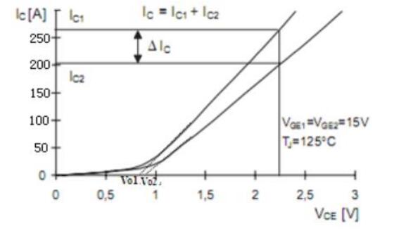
Figure 1 The IGBT situation after the average flow in parallel with different output characteristics
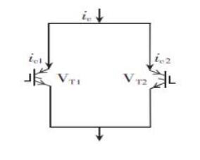
Figure 2 Schematic diagram of the average flow when connected in parallel
The V shown in Figure 1T1And VT2For two identical IGBT models in parallel, Figure 2 shows that the output characteristics of the two IGBT's are slightly different.iC1And iC2respectively VT1And VT2In having the same tube pressure drop (UCE1=UCE2) The collector current below, I indicates the rated current of this type of IGBT, Vcesat1And Vcesat2Represents ote the saturated pressure drop of two I GBT at rated current.It can be approximate that:
R1=(Vce sa t 1-Vo1)/I (1)
R2=(Vce sa t 2-Vo2)/I (2)
UCE1=Vo1+R1×iC1(3)
UCE2=Vo2+R2×iC2(4)
When connected in parallel, the UCE1=UCE2=Uce,Is
iC1=( Uce-Vo1 )/R1=( Uce-Vo1 )×I/(Vcesat1-Vo1)
iC2=(Uce-Vo2)/R1=(Uce-Vo2) ×I/(Vcesat2-Vo2)
Since these two IGBT's are of the same type, Vo1 Vo2 =Vo then
Therefore, if the current of two parallel I GBT modules is I, the current of two IGBT module with different Vce can be calculated as follows:
iC 1=( Uce-V o1 )/R 1=( Uce-V o1 )×I/(Vcesa t 1-V o1)=(Uce-V o )×I/(Vcesa t 1-V o ) iC 2=(Uc e-V o2)/R 1=(Uc e-V o2)×I/(Vc e s a t 2-V o2)=(Uc e-V o )×I/(Vc e s a t 2-V o )
Take the most common GD200HFL120C2S, for example:
Suppose a larger value of Vcesat1 2.5V (125℃), smaller value Vcesat2For 2.1V, (125℃),
Vo =0.8V

Assuming a larger value of Vcesat1Is 2.2V, with the smaller value of Vcesat1For 2.1V, be checked by the data manual
The typical Vo to is =0.8V

If the Vcesat difference is 0.1V, even if the output current required by the parallel module is io =200A, the current difference of the lower IGBT module of another Vce (sat) is 6A.In practice, there will be more loss than another IGBT module, although the IGBT chip is in a large current
It has a positive temperature coefficient, so when the two I GB T modules are in parallel, it is recommended that the difference between V ce (sa t) should not exceed 0.2V. If unavoidable, it is recommended to leave a large margin on the steady state temperature to compensate.
2) Uneven shunt caused by the impedance asymmetry of the power circuit
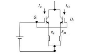
Fig. 2 Effect of impedance of main circuit circuit
It is generally believed that the difference in the parallel line storage of the bus will result in the circuit impedance. Therefore, if the IGBT module using V c e (s a t) difference is less than 0.2V, the symmetry of the bus line must be taken into account. In fact, the impact of this part is actually low, such as the equivalent circuit diagram 2, the RE1And RE2Equivalent to the serial connection of two resistors and the original two uniform flow average branch, if the impedance is inconsistent, it will cause the uniform flow is inconsistent, such as RE1> RE2, That Yao RE2There will inevitably be more current above the branch, causing uneven imbalance and vice versa.Take GD200HFL120C2S as an example:
The actual current required for the parallel module is i o =200A, each module is actually 100A, and the pressure drop on the actual module is Uce =1.7V
Suppose the bronze medal cross-section is 410-5m2, The master row length of module 1 is 0.8m, the master row length of module 1 is 0.6m, and the thermal resistance rate at 30℃ is 1.810-8Ω *m

Compared to the influence of V c e (s a t), the influence of power loop asymmetry is relatively unnecessary when static apprehensive.However, the bus will also introduce the lead inductance, which will have a great impact on the dynamic average flow, which will be further discussed in the future.
3) Influence of the gate pole drive voltage Vge
current ICThe module flowing through the IGBT driven by the gate voltage Vge generates the conduction pressure drop Vce, which is not only related to the flowing current Ic, the V ce (sat) provided above, but also directly related to the gate drive voltage Vge.
Conversely, at different drive voltage Vge, with the same Vce in parallel, the current Ic through the two is naturally different.
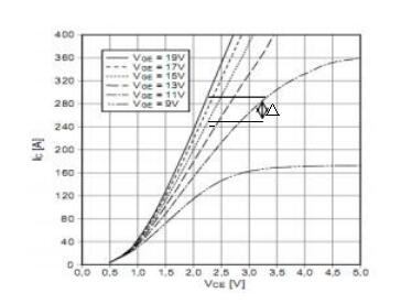
Figure 3. Output characteristic curve of the IGBT module
From Figure 3, we can clearly see that,
As in Vge =13V, at Vce =2.5V, through the current Ic 255A
As in Vge =15V, at Vce =2.5V, through the current Ic 285A

Therefore, the drive circuit design needs to pay very much attention, and be sure to ensure the drive voltage of the parallel module.
It should be emphasized here that the gate voltage Vge discussed above refers to the two ends of the IGBT gate, not the output voltage of the drive plate, and careless customers often make this mistake.As can be seen from Figure 4, there is a gate resistance between the drive chip and the gate pole, and the electrical connection from the drive chip to the I GBT gate pole, which is the gate lead of the machine usually seen on the machine, and the parameter difference of the drive component and the gate lead will be compared with the moment of opening and closing
Highlight, will cause the added to the IGBT gate voltage and the output voltage inconsistency.This will not be a problem in the steady state because the gate belongs to a high resistance state.
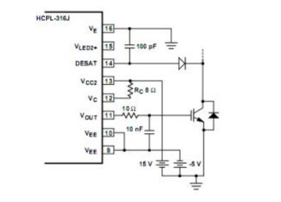
Figure 4 Schematic diagram of the module driver
4) Effect of the open voltage, Vth
Because the voltage applied by the voltage of the drive circuit to the gate is a process from the negative pressure to the applied positive voltage (if there is a negative pressure off), the current I cannot flow through the module before the gate voltage Vth, so the IGBT of the smaller Vge (th) will open earlier and turn off later.Since this effect is mainly at the moment of opening, and it can be known from the transfer characteristic curve of FIG. 4, the I c current is very small when the drive voltage is V t h. Generally, the difference of module Vth of the same type is within 0.5V, so the effect of opening voltage Vth is relatively weak.
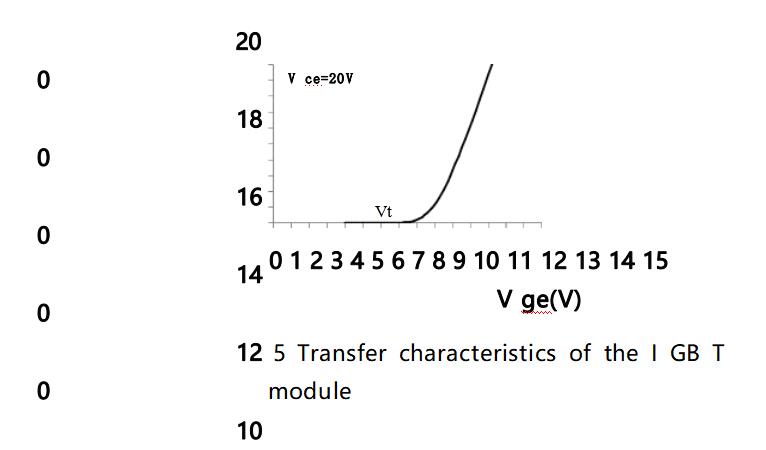
5 Transfer characteristics of the I GB T module
5) Effect of the diode Vf
In the inverter and other applications, the IGB T module reverse parallel diode needs to bear a lot current.The effect of Vf of the diode on the mean flow is exactly the same as that of Vce (sat) on the mean flow, only the I GB T affected by V ce (sat) and the V f of the diode.
R1=(V f-Vo1)/I R2=(V f-Vo2)/I Uf1=Vo1+R1×if1Uf2=Vo2+R2×if2
(1)
(2)
(3)
(4)
When Uf1=Uf2=Uf is connected in parallel, then
iC1=( Uf-Vo1 )/R1=( Uf-Vo1 )×I/(Vf1-Vo1)
iC2=( Uf-Vo2)/R1=( Uf-Vo2) ×I/(Vf2-Vo2)
Since these two diodes are of the same type, Vo1 Vo2 =Vo
Therefore, if the current of two parallel IGBT modules is I, the current of two IGBT module with different Vce can be calculated as follows:
iC1=( Uf-Vo1 )/R1=( Uf-Vo1 )×I/(Vf1-Vo1)=( Uf-Vo ) ×I/(Vf1-Vo) iC12=(Uf-Vo2) / R2= (Uf-Vo2) I / (Vf2-Vo2) = (Uf-Vo) I / (Vf2-Vo) Common 150A module is column,
Assuming that the larger value V f is 2.2V and the smaller value Vf is 2.1V, the typical Vo found by the data manual is =1.3V
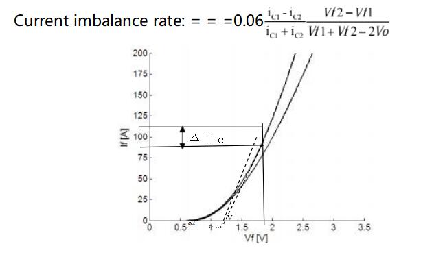
Factors affecting parallel dynamic flow
The main reasons affecting the parallel dynamic mean flow of modules are the following 3 points
A) Dynamic parameters of the IGBT itself
The b) parasitic induction of the drive circuit
c) The parasitic inductance of the power circuit
1) Uneven distribution caused by I GB T's own parameters
The main factor affecting the current equilibrium at the switching time is the transfer characteristics of the parallel device.
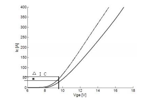
Figure 3. Comparison of the transfer characteristics of the parallel modules
Comparison diagram of two parallel module properties with inconsistent transfer characteristics shown in Figure 3.In FIG. 3, when the same drive voltage V is applied to the parallel moduleGEWhen, the steep IGBT module will withstand more current, and the switching loss will also become larger.2) Parasitism of the drive circuit and uneven shunt caused by the inductance
Combined with the gate-level parasitic capacitance of the IGBT, the parasitic inductance of the driving circuit may cause severe oscillations, causing fluctuations in the gate voltage.The parasitic inductance of the emitter can cause the switching degree variation.
IGBT gate pole drive circuit RG, lead inductance LGLE,, and IGBT input capacitance CinThe process of opening and switching is a typical R L C series circuit response.In Figure 4, the resistor R corresponds to RG, L, corresponding to the inductor LG+LE, Capacitor C corresponds to the input capacitor Cin.![]()
![]()
![]()
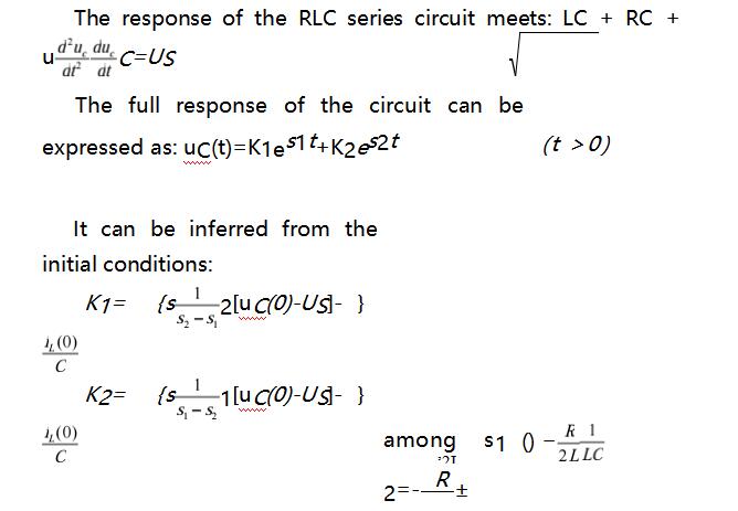
For the on and off process, just uC(0) And the USThe difference of the value of the 1920s, when turned on, uC(0)=-10V ,US=15V (the general drive voltage is often + 15V on, -10V off), and when off, uC(0)=15V ,US=-10V

Due to the parasitic lead inductance of LGLEThe existence, will increase the possibility of gate pole shock, need to avoid the generation of this lead inductance.In the actual line, the length of the gate lead and the area of the gate lead loop (such as a twisted pair) can be reduced.While the gate electrode resistance, RGIt needs to be added separately to start up with better results.
![]()
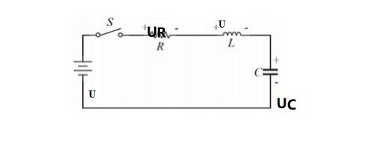
Figure 4 Transmitter-parasitic inductance of the drive circuit
3) Uneven distribution caused by the parasitic inductance of the power circuit
The parasitic inductor of the power circuit mainly consists of two main parts, namely, the collector parasitic inductor Lc
And the emitter-parasitic inductor Le, as shown in Figure 5. When the gate voltage drive waveform is switched, the power loop is being rapidly changing, and the speed is at a subtle level. The inductors L c and L e of the power loop will play a role in hindering the change of current, resulting in the slow conversion speed.In parallel, due to the relationship between layout and wiring, there are great differences in the parasitic inductance of the power circuit, which is bound to cause dynamic diversion imbalance.Here especially emphasize the collector parasitic inductor L c, due to the parallel current is very large, the current is off, because the off speed, current is very large, collector parasitic inductor Lc tend to produce large and bus voltage direction reverse momentum, and bus voltage superposition on IGBT above IGBT, impact, if more than IG BT rated voltage, is bound to cause damage to IGBT.
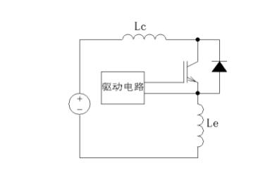
Figure 5. Parasitic inductance of the power circuit
Therefore, designers need to optimize the circuit design of the main circuit according to the actual conditions. For example, if the copper row can be used, not copper wire, if the cost allows, adopt the main loop mode.
1) Selection of modules
From the static flow, N PT IGBT module has positive temperature coefficient is suitable for parallel.On the other hand, parallel modules, especially those on the same bridge arm, can use the same batch of modules as far as possible, so as to ensure the consistency of parameters to the maximum extent.
2) Drive loop design
When the IGBT module is in parallel, influenced by the inductance of the gate circuit wiring and the input capacitor of IGBT, the gate voltage sometimes rises. In order to prevent this oscillation, the gate resistance should be connected on the IGBT gate.
When the emitter wiring of the driving circuit is connected at a different position from the main circuit, the transient current distribution of the parallel-connected IGBT becomes unbalanced.The IGBT module has the auxiliary emission extremes used by the drive circuit, be sure to use this terminal,
The driving wiring can be equal, and the transient current imbalance caused by the wiring method of the driving circuit can be suppressed.
Door-pole wiring is also critical:
A) The drive line should be short, and the effect of the twisted pair line will be better;
b) The drive line should be far away from the main circuit, try to achieve orthogonal layout;
c) Each drive line moves separately and is not tied together.
3) Line layout
When the resistance part and the inductance part of the main circuit wiring are unequal, the current distribution of the parallel connected elements will produce uneven uniform flow.In addition, if the inductance parasitic by the main circuit is large, the surge voltage will increase when IGBT is turned off. Therefore, in order to reduce the inductance of the circuit, the parallel connected IGBT module should be configured as closely as possible, and the wiring should maintain good symmetry.
In order to reduce the line sense and line resistance, the DC bus to avoid using cable wire, this wire self-sensing and mutual sense are very poor, and the thermal conductivity is very poor.Copper strip can effectively solve the self-perception and heat dissipation, but the mutual feeling is still very large.Laminated bus is multi-layer copper plate stacked together, layer and layer directly using insulation heat conductivity isolation, effectively solve the self-sensing, mutual sense, heat dissipation, but also has the role of impedance and reduce E M I, is a relatively ideal bus form, as shown in the figure below:
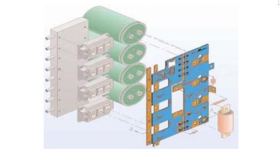
Figure 6 layer stacked bus diagram
In addition, the modules should be mounted on the same radiator close to each other to obtain optimal thermal coupling with uniform temperature and minimize the effects of Tj and Vth.
conclusion:
This paper analyzes the factors affecting the average flow of parallel modules, combined with Star's equipment, in addition to providing products more suitable for parallel, but also proposes the attention of using IGBT modules for parallel design from the perspective of application, so that designers can have a deeper understanding of IGBT parallel and can follow the design.
reference documentation:
1.I n t e r n a ti on a l R ec tifi e r A pp li ca ti on N o t e s .AN 990. A pp li ca ti on C ha r ac t e ri za ti on o f I GB T s [ Z ] ,2002.
2.D yn e x S e m i c ondu c t o r .AN 5505. P a r a ll e l O p e r a ti on o f D yn e x IGBT M odu l e s[Z ] ,2001.
3 Sun Qiang, Wang Xueru, Cao Yuelong, high-power IGBT module parallel average flow problem research [J] Power electronics technology in 2004
4. Tong Shi Bai Hua Chengying simulation electronic technology foundation [M].Higher Education Press, 2001
LET'S GET IN TOUCH

Privacy statement: Your privacy is very important to Us. Our company promises not to disclose your personal information to any external company with out your explicit permission.

Fill in more information so that we can get in touch with you faster
Privacy statement: Your privacy is very important to Us. Our company promises not to disclose your personal information to any external company with out your explicit permission.