


Please Leave Us A Message
Privacy statement: Your privacy is very important to Us. Our company promises not to disclose your personal information to any external company with out your explicit permission.

 April 19, 2019
Gallium nitride (GaN) field-effect transistors have the advantage of high switching speeds and require good measurement techniques and good techniques for describing high-speed waveform details. This article focuses on how to accurately evaluate high-performance GaN transistors using measurement equipment based on user requirements and measurement techniques. In addition, this article evaluates the case when a high-bandwidth differential probe is used with an ungrounded reference waveform.
To illustrate the measurement techniques and requirements for various GaN power devices, we use the following EPC GaN field-effect transistors (eGaN FETs): (i) High-speed, 10MHz switching frequency, 65V eGaN FET-based EPC8009 half-bridge development board (Q1 and Q2 of Figure 1); and (ii) the EPC9080 half-bridge demo board with a low-speed, 500kHz switching frequency using a 100V eGaN FET EPC2045 as the top switch (Q1) and 100V EPC2022 as the bottom switch (Q2) device. As shown in Figure 1, both boards are configured as buck converters.

Figure 1: Simplified schematic of the eGaN FET test board used in this article
The maximum bandwidth of the oscilloscope and probe system is given by [1]:
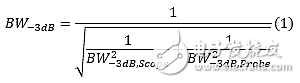
Among them, BW-3dB, BW-3dB, Scope and BW-3dB, Probe is the bandwidth (in Hz) of the system, oscilloscope and probe respectively. This article uses a 2GHz oscilloscope (Tektronix MSO 5204). The passive probe (Tektronix TPP1000) has a maximum bandwidth of 1 GHz. The lower bandwidth (1 GHz) between the oscilloscope and the probe has a greater impact on system bandwidth.
When evaluating the layout of a PCB design, typical measurements include rise and fall times, peak overshoot, undershoot, and expected switching node rising edge ringing frequencies, which can be estimated by using the ringing frequency equation:
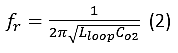
In Equation 2, Lloop is a high-frequency loop inductor consisting of a high-frequency decoupling capacitor, eGaN FETs (Q1 and Q2), and components connected to the PCB. Co2 = Coss + Cpar contains Coss, which is the output capacitance of the bottom side FET Q2 at Q2 blocking voltage. Cpar is the parasitic and probe capacitance at the switch node. The Lloop of the demo board used in this paper is estimated to be approximately 200-300 pH [2]. The EPC8009 has a Coss of 30pF [3] over the test voltage range, and the Cpar of this demo board is approximately 10pF. This shows the ringing frequency of fr1~1.6GHz. The design based on EPC2045 and EPC2022 has a large capacitance, and the ringing frequency is estimated to be fr2~0.44GHz.
It is clear from [1] that the highest system bandwidth available is lower than the ringing frequency of the EPC8009 based design. Now we will observe how choosing different system bandwidths affects the switching node waveforms of higher speed GaN transistors (such as EPC8009) and relatively slower GaN transistors (such as EPC2045 and EPC2022).
The measurement system acts like a low-pass filter that attenuates the high frequency portion as shown in Figure 2 (top). As seen in Figure 2, the rise time of the waveform is significantly different. This can be attributed to the relationship between system bandwidth and rise time according to the following equation [1]:
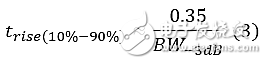
The fastest rise time of Figure 2 (left) is approximately 0.4 ns, corresponding to a system bandwidth of ~1 GHz. Using the same probe and oscilloscope with a 500MHz bandwidth digital filter, the measured rise time is 0.8ns. Obviously, the rise time of the signal is limited by the system bandwidth. Since the measured rise time is equal to the calculated system rise time, the input signal is faster than the rise time of the measurement system. Therefore, the input signal rise time may be much lower than 0.4 ns.
The ringing frequency (fr1) measured by the design of the EPC8009 is 1.176 GHz, which uses a probe with a maximum bandwidth of 1 GHz. The lower bandwidth condition shown in Figure 2 (top) further reduces the accuracy of measuring the ringing frequency. When considering peak voltage overshoot, it is also apparent that lower bandwidth measurements underestimate the peak voltage of each switching device. System bandwidth is also important for timing-dependent dead time measurements. As shown in Figure 2 (top), the dead time is visible for the 500MHz and 1GHz bandwidths, although the measurements are not very accurate. At lower bandwidths, dead time is almost non-existent. Table 1 shows the effect of system bandwidth on key measurements using the highest speed EPC8009.
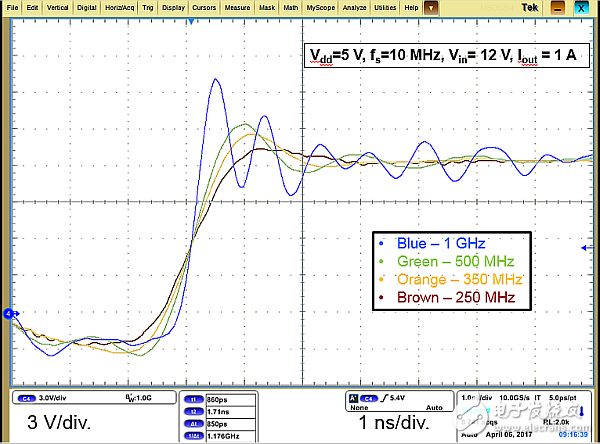
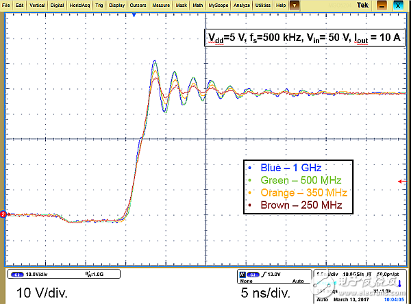
Figure 2: Effect of probe/system bandwidth on the waveform (top is based on the EPC8009 board and bottom is based on the EPC9080 board)
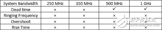
Table 1: measurable parameters (based on EPC8009 board)
Another test case was demonstrated with the EPC9080 demo board, which has a much lower ringing frequency and switching speed due to the lower on-resistance and higher capacitance of the on-board eGaN FET [4]. The corresponding waveform is shown in Figure 2 (below). Since fr2 is lower than the system's -3dB frequency, the 438MHz ringing frequency (fr2) and its amplitude measured using the 1GHz (blue) probe are correct. The 1GHz (blue) and 500MHz (green) waveforms capture all the details accurately. But for system bandwidths of 350MHz (orange) and 250MHz (brown), fr2 is higher than the system bandwidth. Therefore, it captures the shape of the ringing waveform, but significantly reduces the ringing, thus underestimating the overshoot. The rise time measured for different system bandwidths is approximately 3 ns. According to (2), the lowest bandwidth we use is 250MHz, which corresponds to a rise time of 1.6ns, and the rise time in all cases can be accurately measured. Table 2 summarizes.
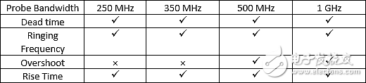
Table 2: Measurable parameters (EPC9080)
In the second part of this article, we will show how to use good probe technology and the importance of choosing measurement points to generate high fidelity and accurate waveforms.
1. Use a probe with a low input capacitance and keep the ground as short as possibleTwo types of probe grounding schemes for passive probes (Tektronix TPP 1000): alligator clips and spring clips [5] (Figure 3).
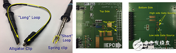
Figure 3: Different probe technologies
Longer ground leads are convenient because the user can make a ground connection and detect multiple test points within the ground lead range. However, any one of the wires has a distributed inductance, and the distributed inductance becomes more and more obstructive to the AC signal as the signal frequency increases. The inductance of the ground lead interacts with the probe input capacitance to produce ringing at a specific frequency (see Equation 2). This ringing is unavoidable and may be seen as a sinusoid that attenuates the amplitude. As the length of the ground wire increases, the inductance increases and the signal under test will ring at a lower frequency.
This section uses the EPC9080 half-bridge demo board for measurement techniques. The switching node waveform is measured at two points as shown in Figure 3: "near point" near the FET switch node; and "far point" at the PCB peripheral pin terminals. Figure 4 shows the waveforms of each probe point and the switching node (VSW) measured with the probe technique.
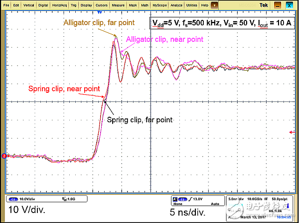
Figure 4: Probe technology and the effect of selecting different measurement points
The measured waveform of Figure 4 clearly shows that probe technology is more important than the choice of measurement points. Although there is edge attenuation, the red and black waveforms are almost identical. Regardless of the choice of measurement points, the shape of the waveform when using the alligator clip is very inaccurate. We recommend that the spring clip technology be used in conjunction with the measurement point closest to the power device ("near point").
2. Ungrounded reference high frequency measurement using an isolated measurement systemDifferential measurements describe any measurement between two test points, but the term is most commonly used when describing measurements involving ungrounded reference test points. Several common methods of measuring differential signals are: (a) calculating two single-ended probes and an oscilloscope to measure the difference; (b) using a high-bandwidth, high-voltage differential probe; and (c) using an isolated measurement scheme [6].
First consider the method of using a mathematical function in an oscilloscope to measure the voltage of two selected test points using two ground reference probes. Then, the difference between the two voltage waveforms is displayed in a mathematical waveform. The differential math waveform is a pseudo differential measurement. Although limited in performance, this technique may be sufficient to handle low frequency measurements with low common mode signals. For proper operation, both inputs must be set to have the same scale factor, and the probes must be the same model and match very well. Any mismatch between the probe's attenuation/gain, propagation delay, and mid-high frequency response will result in less accurate measurements. Common mode rejection ratio (CMRR) performs very poorly at higher frequencies, while large common mode signals can cause oscilloscope input to be out of tune.
The best method for accurate differential measurements is a high performance, isolated measurement solution such as the Tektronix IsoVu measurement system. In a half bridge circuit such as having a large common mode voltage and a fast edge rate, a signal such as a high side gate-source voltage cannot be measured without a high performance CMRR at high frequencies. Although conventional differential probes have better common-mode rejection at frequencies as low as a few MHz, CMRR performance is significantly reduced at frequencies above a few MHz. Isolation systems such as Tektronix IsoVu enable high performance CMRR at high frequencies.
Figure 5 shows the difference between the oscilloscope math and the isolated measurement system for the high side gate-source signal (VGS1) of the EPC9080 board (Figure 1).
The high switching noise in a "noisy" environment amplifies the difference between measurements when the circuit is powered by the voltage and current shown. Due to its high CMRR, the waveform captured using the isolation probe is clearer [7].
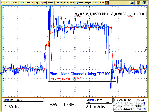
Figure 5: High Side Grid-Source VGS1 Waveform (Noise Environment)
This article describes the measurement of various EPC-based GaN field-effect transistor (eGaN FET) power converters, including bandwidth effects, probe technology, and the appropriate use of high-bandwidth isolation probes. For specific applications, circuit designers who can use better measurement techniques and techniques and learn more about measurement system requirements can maximize the performance of their GaN-based designs.
The above is the How to use measurement equipment to accurately evaluate high performance GaN transistors we have listed for you. You can submit the following form to obtain more industry information we provide for you.
You can visit our website or contact us, and we will provide the latest consultation and solutions
Send Inquiry
Most Popular
lastest New
Send Inquiry
Tel: 86-514-87782298
Whatsapp: +8613805278321
Address: 3rd Floor, Weiheng Building No.20 B Area, Yangzhou, Jiangsu China
Website: https://www.yzpst.com
Privacy statement: Your privacy is very important to Us. Our company promises not to disclose your personal information to any external company with out your explicit permission.
Fill in more information so that we can get in touch with you faster
Privacy statement: Your privacy is very important to Us. Our company promises not to disclose your personal information to any external company with out your explicit permission.