


Please Leave Us A Message
Privacy statement: Your privacy is very important to Us. Our company promises not to disclose your personal information to any external company with out your explicit permission.

 December 15, 2020
The design of any high performance ADC, especially the RF sampling ADC, input or front end, is critical to achieve the required system level performance. In many cases, RF sampling ADCs can digitally quantize signal bandwidths of hundreds of MHz. The front end can be active (using amplifiers) or passive (using transformers or baluns), depending on the system requirements. In either case, components must be carefully selected to achieve optimal ADC performance at the target frequency band.
IntroductionRF sampling ADCs are fabricated using deep sub-micron CMOS process technology, and the physical characteristics of semiconductor devices indicate that smaller transistor sizes support lower maximum voltages. Therefore, in the data book specifies the absolute maximum voltage that should not be exceeded for reasons of reliability, compared with the current mainstream RF sampling ADC, it can be found that this voltage value is smaller.
In receiver applications where the ADC is used to digitally quantize the input signal, system designers must pay close attention to the absolute maximum input voltage. This parameter directly affects the lifetime and reliability of the ADC. Unreliable ADCs may render the entire radio system unusable and the replacement cost may be very large.
To counteract the risk of overvoltage, the RF sampling ADC integrates a circuit that can detect high-level thresholds, allowing the receiver to compensate for gain adjustment through an automatic gain control (AGC) loop. However, if a pipelined ADC is used, the inherent architecture-related delays may cause the input to be exposed to high levels, potentially damaging the ADC input. This article discusses a simple way to enhance the AGC loop and protect the ADC.
Input schemaRF sampling ADCs can use a variety of different designs. The most common one is a pipeline architecture that uses multiple cascades to convert analog signals to digital signals. The first level is the most important and can be buffered or unbuffered. Which design to choose depends on design requirements and performance goals. For example, a buffered ADC typically has better SFDR performance in the frequency range but consumes more power than an unbuffered ADC.
The front-end design will also change depending on whether the ADC has a buffer stage. ADCs without buffers require additional series resistors to handle the input charge kickback, which also improves SFDR performance. Figure 1 and Figure 2 show a simplified diagram of the equivalent input circuit for the AD9625 unbuffered and AD9680 buffered RF sampling ADC. For simplicity, only single-ended inputs are shown.

Figure 1. Equivalent circuit of unbuffered RF sampling ADC input
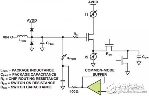
Figure 2. Equivalent circuit for buffering RF sampling ADC input
Regardless of the architecture, the absolute maximum absolute voltage at the ADC input is determined by the voltage that the MOSFET can handle. Buffered inputs are more complex and consume more power than unbuffered inputs. ADCs have many different types of buffers, the most common being source followers.
Failure mechanismThe fault mechanisms for buffered and unbuffered ADCs are different, but typically fail when the maximum allowable gate-source voltage ((VGS)) or drain-source voltage (VDS) is exceeded. These voltages are shown in Figure 3.

Figure 3. Key voltages of MOS transistors
For example, assuming that the VDS exceeds the maximum voltage allowed, a VDS breakdown fault occurs, which typically occurs when the MOSFET is in an off state and an excessive voltage with respect to the source is applied to the drain. If VGS exceeds the maximum voltage allowed, it can cause VGS breakdown (also called oxide breakdown). This usually occurs when the MOSFET is in a conducting state and an excessive voltage with respect to the source is applied to the gate.
Unbuffered ADC failure mechanismFigure 4 shows an unbuffered ADC input. The sampling process is controlled by the inverted clock signals Φ and Φ, which are the sample/hold signal of the MOSFET M1 and the reset signal of the MOSFET M2. When M1 turns on, M2 turns off and capacitor CSW tracks the signal (sampling or tracking mode). When M1 turns off, the comparator in MDAC makes a decision and M2 turns on, and capacitor CSW resets. This prepares the sampling capacitor for the next sample in the sampling phase. This circuit is usually in good working condition.
However, the high voltage input exposes M2 to a stress that exceeds its drain-source voltage. When the input high voltage is sampled (M1 on, M2 off), M2 is exposed to a large VDS, which is off for less than half of the sample clock, but even if it is only transient exposure. This will degrade the reliability of the circuit and cause the ADC to fail over time. In reset mode (M1 is off, M2 is on), there is an input signal on the drain of M1, which is exposed to a large VDS voltage.

Figure 4. Failure Mode of Unbuffered ADC Input
Buffered ADC failure mechanismFigure 5 shows a buffered ADC input. The same clocking scheme applies to the sample and reset signals. Regardless of the phase, currents I1 and I2 are generated when the gate of buffer M3 is exposed to a high voltage input. The current source I1 is implemented using PMOS transistors, and I2 is implemented using NMOS transistors. The high voltage on the M3 gate causes excessive VDS in the I1 and I2 MOSFETs. In addition, the high voltage on the M3 gate can also cause breakdown of the oxide layer.

Figure 5. Buffering ADC Input Fault Mode
The breakdown mechanism of buffered and unbuffered ADCs is different, so the absolute maximum input voltage is also different, as shown in Table 1.
The above is the Schottky diode protection RF sampling ADC input we have listed for you. You can submit the following form to obtain more industry information we provide for you.
You can visit our website or contact us, and we will provide the latest consultation and solutions
Send Inquiry
Most Popular
lastest New
Related Products
Send Inquiry
Tel: 86-514-87782298
Whatsapp: +8613805278321
Address: 3rd Floor, Weiheng Building No.20 B Area, Yangzhou, Jiangsu China
Website: https://www.yzpst.com
Privacy statement: Your privacy is very important to Us. Our company promises not to disclose your personal information to any external company with out your explicit permission.
Fill in more information so that we can get in touch with you faster
Privacy statement: Your privacy is very important to Us. Our company promises not to disclose your personal information to any external company with out your explicit permission.